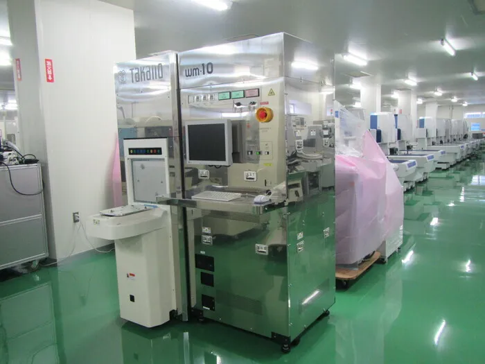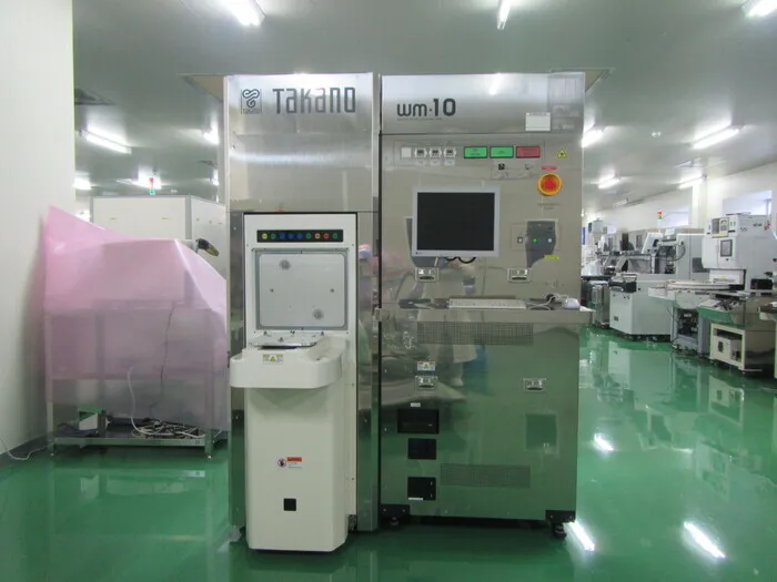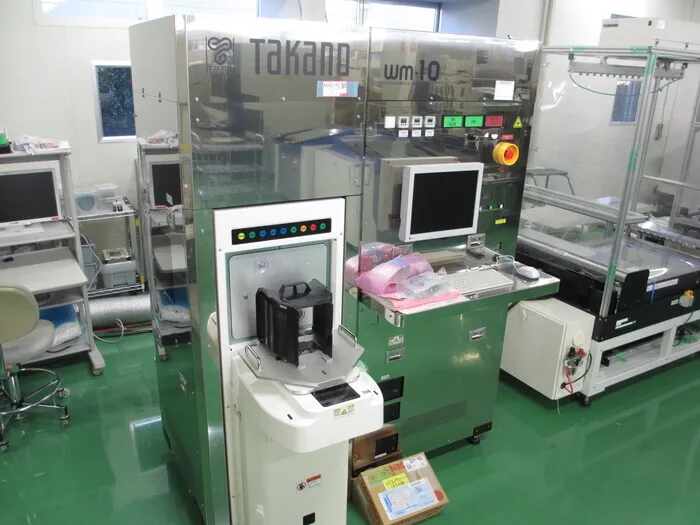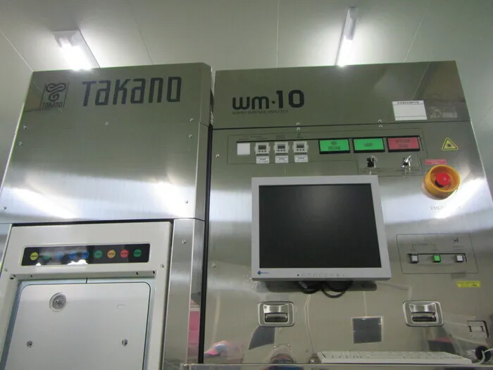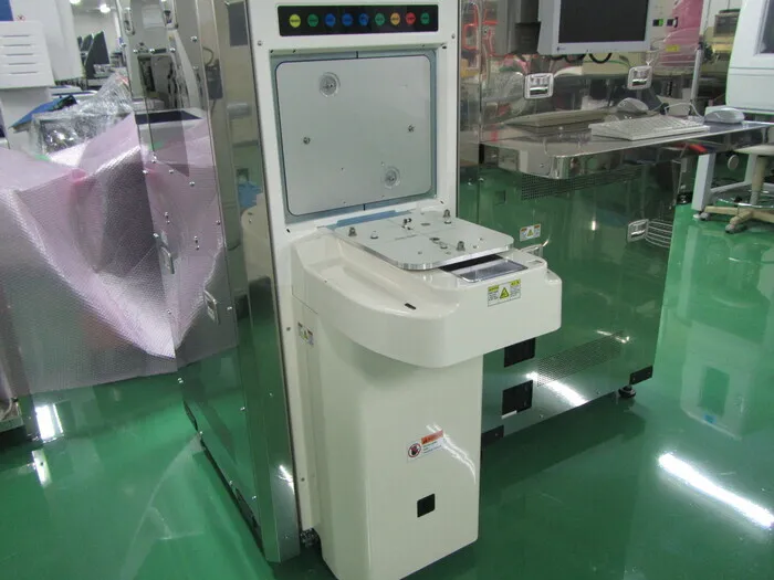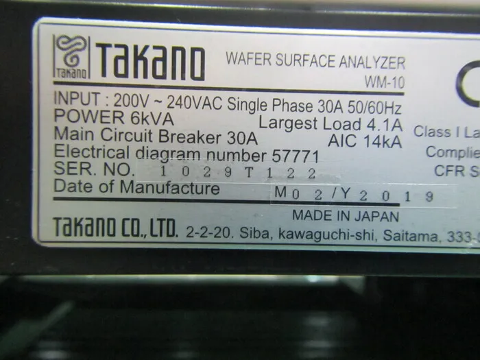



Wafer surface inspection equipment - Takano WM-10
Product Specifications
Maker Takano
Model WM-10
Category Semiconductor (Post-process)
Model year 2019
External Dimensions W1272 D1213 H1650
Condition Used
Showroom Information
Exhibition hall Enzan Technical Center
Price & Inquiry
price Price Inquiry
Inquiry Number MA0110
Mechanical Specifications
Features: High-output Violet-LD, maximum detection sensitivity of 48 nm
Ideal for mass production and prototyping of 90 to 65 nm process nodes
Light source: VioletLD
Detection/scanning method: Scattered light detection/spiral scanning method
Scattered light detection/spiral scanning method: Bare 48 nm/Film 60 nm
Wafer size: 300/200mm compatible
Input power: 1φ200-240V 50/60Hz 30A
Attachments
Product Overview
Takano WM-10 is a used Semiconductor (Post-process) item handled by ASKINDEX Korea. External dimensions: W1272 D1213 H1650. This listing has sold, but you can ask about restock or a similar unit, and request a quote. You can also compare other used products from the same manufacturer (Takano) and the same category (Semiconductor (Post-process)).
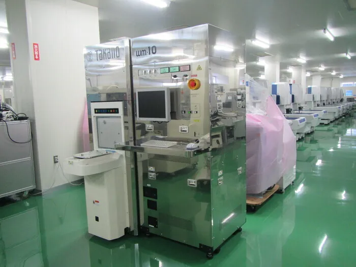
※ Click on the image below to zoom in.